- 您现在的位置:买卖IC网 > Sheet目录2006 > LTC2642IDD-16#PBF (Linear Technology)IC DAC 16BIT VOUT 10-DFN
LTC2641/LTC2642
4
26412fc
For more information www.linear.com/LTC2641
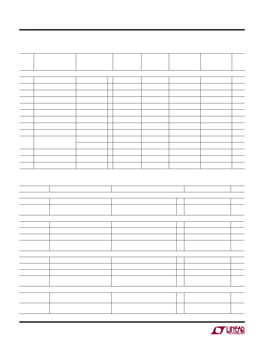
elecTrical characTerisTics
SYMBOL
PARAMETER
CONDITIONS
MIN
TYP
MAX
UNITS
Reference Input
VREF
Reference Input Range
l
2.0
VDD
V
RREF
Reference Input Resistance (Note 5)
Unipolar Mode (LTC2641)
Bipolar Mode (LTC2642)
l
11
8.5
14.8
11.4
k
Ω
k
Ω
Dynamic Performance—VOUT
SR
Voltage Output Slew Rate
Measured from 10% to 90%
15
V/s
Output Settling Time
To ±0.5LSB of FS
1
s
DAC Glitch Impulse
Major Carry Transition
0.5
nVs
Digital Feedthrough
Code = 0000hex; NCS = VDD;
SCLK, DIN 0V to VDD Levels
0.2
nVs
Dynamic Performance—Reference Input
BW
Reference –3dB Bandwidth
Code = FFFFhex
1.3
MHz
Reference Feedthrough
Code = 0000hex, VREF = 1VP-P at 100kHz
1
mVP-P
SNR
Signal-to-Noise Ratio
92
dB
CIN(REF)
Reference Input Capacitance
Code = 0000hex
Code = FFFFhex
75
120
pF
Digital Inputs
VIH
Digital Input High Voltage
VCC = 3.6V to 5.5V
VCC = 2.7V to 3.6V
l
2.4
2.0
V
VIL
Digital Input Low Voltage
VCC = 4.5V to 5.5V
VCC = 2.7V to 4.5V
l
0.8
0.6
V
The l denotes the specifications which apply over the full operating
temperature range, otherwise specifications are at TA = 25°C. VDD = 3V or 5V, VREF = 2.5V, CL = 10pF, GND = 0, RL = ∞unless otherwise
specified.
SYMBOL PARAMETER
CONDITIONS
LTC2641-12
LTC2642-12
LTC2641-14
LTC2642-14
LTC2641-16
LTC2642-16
LTC2641A-16
LTC2642A-16
UNITS
MIN TYP MAX MIN TYP MAX MIN TYP MAX MIN TYP MAX
Static Peformance
N
Resolution
l
12
14
16
Bits
Monotonicity
l
12
14
16
Bits
DNL
Differential Nonlinearity
(Note 3)
l
±0.5
±0.5 ±1
±0.5
±1
±0.5
±1
LSB
INL
Integral Nonlinearity
(Note 3)
l
±0.5
±0.5 ±1
±0.5
±2
±0.5
±1
LSB
ZSE
Zero Code Offset Error
Code = 0
l
1
2
LSB
ZSTC
Zero Code Tempco
±0.05
ppm/°C
GE
Gain Error
l
±0.5 ±2
±1
±4
±2
±5
±2
±5
LSB
GETC
Gain Error Tempco
±0.1
ppm/°C
ROUT
DAC Output Resistance
(Note 4)
6.2
k
Ω
Bipolar Resistor Matching (LTC2642) RFB/RINV
1
Ratio Error (Note 7) l
±0.1
±0.03
±0.015
%
BZE
Bipolar Zero Offset Error
(LTC2642)
l
±0.5 ±2
±0.5 ±4
±2
±5
±2
±5
LSB
BZSTC
Bipolar Zero Tempco
(LTC2642)
±0.1
ppm/°C
PSR
Power Supply Rejection
ΔVDD = ±10%
l
±0.5
±1
LSB
The l denotes the specifications which apply over the full operating temperature range, otherwise specifications are at TA = 25°C.
VDD = 3V or 5V, VREF = 2.5V, CL = 10pF, GND = 0, RL = ∞unless otherwise specified.
发布紧急采购,3分钟左右您将得到回复。
相关PDF资料
LTC2704IGW-16#PBF
IC DAC 16BIT QUAD VOUT 44-SSOP
LTC2751AIUHF-16#PBF
IC DAC 16BIT CUR OUT 38-QFN
LTC2752ACLX#PBF
IC DAC 16BIT DUAL CUR OUT 48LQFP
LTC2753AIUK-16#TRPBF
IC DAC 16BIT DUAL 48-QFN
LTC2754AIUKG-16#PBF
IC DAC 16BIT QUAD IOUT 52-QFN
LTC2755AIUP-16#PBF
IC DAC 16BIT CUR OUT 64-QFN
LTC2757ACLX#PBF
IC DAC 18BIT PAR 48LQFP
LTC2758AILX#PBF
IC DAC 18BIT SPI/SRL 48-LQFP
相关代理商/技术参数
LTC2642IDD-16#TRPBF
功能描述:IC DAC 16BIT VOUT 10-DFN RoHS:是 类别:集成电路 (IC) >> 数据采集 - 数模转换器 系列:- 标准包装:47 系列:- 设置时间:2µs 位数:14 数据接口:并联 转换器数目:1 电压电源:单电源 功率耗散(最大):55µW 工作温度:-40°C ~ 85°C 安装类型:表面贴装 封装/外壳:28-SSOP(0.209",5.30mm 宽) 供应商设备封装:28-SSOP 包装:管件 输出数目和类型:1 电流,单极;1 电流,双极 采样率(每秒):*
LTC2642IMS-12#PBF
功能描述:IC DAC 12BIT VOUT 10-MSOP RoHS:是 类别:集成电路 (IC) >> 数据采集 - 数模转换器 系列:- 产品培训模块:LTC263x 12-, 10-, and 8-Bit VOUT DAC Family 特色产品:LTC2636 - Octal 12-/10-/8-Bit SPI VOUT DACs with 10ppm/°C Reference 标准包装:91 系列:- 设置时间:4µs 位数:10 数据接口:MICROWIRE?,串行,SPI? 转换器数目:8 电压电源:单电源 功率耗散(最大):2.7mW 工作温度:-40°C ~ 85°C 安装类型:表面贴装 封装/外壳:14-WFDFN 裸露焊盘 供应商设备封装:14-DFN-EP(4x3) 包装:管件 输出数目和类型:8 电压,单极 采样率(每秒):*
LTC2642IMS-12#TRPBF
功能描述:IC DAC 12BIT VOUT 10-MSOP RoHS:是 类别:集成电路 (IC) >> 数据采集 - 数模转换器 系列:- 产品培训模块:LTC263x 12-, 10-, and 8-Bit VOUT DAC Family 特色产品:LTC2636 - Octal 12-/10-/8-Bit SPI VOUT DACs with 10ppm/°C Reference 标准包装:91 系列:- 设置时间:4µs 位数:10 数据接口:MICROWIRE?,串行,SPI? 转换器数目:8 电压电源:单电源 功率耗散(最大):2.7mW 工作温度:-40°C ~ 85°C 安装类型:表面贴装 封装/外壳:14-WFDFN 裸露焊盘 供应商设备封装:14-DFN-EP(4x3) 包装:管件 输出数目和类型:8 电压,单极 采样率(每秒):*
LTC2642IMS-14#PBF
功能描述:IC DAC 14BIT VOUT 10-MSOP RoHS:是 类别:集成电路 (IC) >> 数据采集 - 数模转换器 系列:- 标准包装:47 系列:- 设置时间:2µs 位数:14 数据接口:并联 转换器数目:1 电压电源:单电源 功率耗散(最大):55µW 工作温度:-40°C ~ 85°C 安装类型:表面贴装 封装/外壳:28-SSOP(0.209",5.30mm 宽) 供应商设备封装:28-SSOP 包装:管件 输出数目和类型:1 电流,单极;1 电流,双极 采样率(每秒):*
LTC2642IMS-14#TRPBF
功能描述:IC DAC 14BIT VOUT 10-MSOP RoHS:是 类别:集成电路 (IC) >> 数据采集 - 数模转换器 系列:- 标准包装:47 系列:- 设置时间:2µs 位数:14 数据接口:并联 转换器数目:1 电压电源:单电源 功率耗散(最大):55µW 工作温度:-40°C ~ 85°C 安装类型:表面贴装 封装/外壳:28-SSOP(0.209",5.30mm 宽) 供应商设备封装:28-SSOP 包装:管件 输出数目和类型:1 电流,单极;1 电流,双极 采样率(每秒):*
LTC2642IMS-16#PBF
功能描述:IC DAC 16BIT VOUT 10-MSOP RoHS:是 类别:集成电路 (IC) >> 数据采集 - 数模转换器 系列:- 标准包装:1 系列:- 设置时间:4.5µs 位数:12 数据接口:串行,SPI? 转换器数目:1 电压电源:单电源 功率耗散(最大):- 工作温度:-40°C ~ 125°C 安装类型:表面贴装 封装/外壳:8-SOIC(0.154",3.90mm 宽) 供应商设备封装:8-SOICN 包装:剪切带 (CT) 输出数目和类型:1 电压,单极;1 电压,双极 采样率(每秒):* 其它名称:MCP4921T-E/SNCTMCP4921T-E/SNRCTMCP4921T-E/SNRCT-ND
LTC2642IMS-16#TRPBF
功能描述:IC DAC 16BIT VOUT 10-MSOP RoHS:是 类别:集成电路 (IC) >> 数据采集 - 数模转换器 系列:- 标准包装:47 系列:- 设置时间:2µs 位数:14 数据接口:并联 转换器数目:1 电压电源:单电源 功率耗散(最大):55µW 工作温度:-40°C ~ 85°C 安装类型:表面贴装 封装/外壳:28-SSOP(0.209",5.30mm 宽) 供应商设备封装:28-SSOP 包装:管件 输出数目和类型:1 电流,单极;1 电流,双极 采样率(每秒):*
LTC-2651TBE-01
制造商:LITEON 功能描述:8*4 ND, 0.28 inch, common anode, color-blue